Mission-critical PCB Design
and Manufacturing at Global Scale
Moving 224G mSAP Interconnects from Design Theory to High-Volume Production
Standard fabrication methods hit physical limits at next-generation speeds. Sanmina bypasses these barriers with proprietary additive processing that ensures perfectly vertical sidewalls and precise geometry. We industrialize these complex architectures to move you from domestic prototype to global volume without re-engineering.
-
Physics-Grade Signal Clarity (224G Ready)
-
Secure US NPI & Global Footprint
-
Flight-Ready Hardware Validation
-
Direct Access to mSAP Engineering Leads

mSAP Additive Processing
2 mil line / 2 mil space for
0.3mm pitch
Extreme Fabrication Complexity
>90 Layer counts and
400 mil thickness
Secure Domestic Fabrication
ITAR and AS9100 certified in our
US facilities
Global Volume Scale
Automated high-density production in
worldwide facilities
Meet the team

Steve Bray
VP of Field Applications Engineering, PCB Division
(209) 275-3726
steve.bray@sanmina.com
Resolve the 224G Signal Integrity Bottleneck
Meet with Steve to review mSAP qualification data, vertical sidewall physics, and optical backdrilling tolerances for zero-stub architectures. We will audit your stack-up to ensure your high-speed simulations translate into a manufacturable reality.

Zeljko Sola
SVP of PCB Global Sales Technology & Commercial Sector
(408) 964-4656
zeljko.sola@sanmina.com
Accelerate Your Global PCB Supply Chain
Meet with Zeljko to audit your production roadmap and ensure global yield continuity. We will map a seamless move from domestic NPI to automated volume centers, ensuring your 224G innovation scales without compromise.
Engineering Complexity • Mastering Precision • Scaling Globally

Layer Density
>90 Layers proven in ruggedized defense backplanes
Circuit Precision
2 mil / 2 mil line and space via mSAP additive processing
Form Factor
28″ x 42″ large format panel capability
Material Qualification
Ultra-Low Loss for Panasonic MEG8 and EMC EM892K2
Precision Drilling
Optical Backdrilling with advanced ±2 mil stub tolerances
Thermal & Power
Heavy Copper >6 oz for high-current automotive and industrial power
Flexible Worldwide Capabilities for NPI and Volume Production
IP Security and High-Mix Complexity
ITAR, EAR, Defense, and Flex / Rigid-Flex Architectures
Automated Precision and High Volume
Advanced HDI, Automotive Reliability, and High-Speed Computing

IP Security and High-Mix Complexity
ITAR, EAR, Defense, and Flex / Rigid-Flex Architectures
Automated Precision and High Volume
Advanced HDI, Automotive Reliability, and High-Speed Computing
Validated Performance Across Multiple Industries

DEFENSE + AEROSPACE
Ruggedized Precision
AS9100 certified reliability for mission-critical backplanes and radar systems.
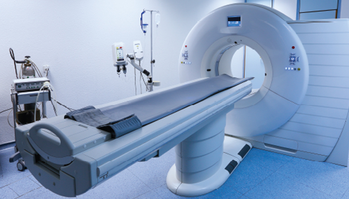
MEDICAL + INDUSTRIAL
Lifecycle Reliability
ISO 13485 fabrication for diagnostic imaging and surgical robotics.

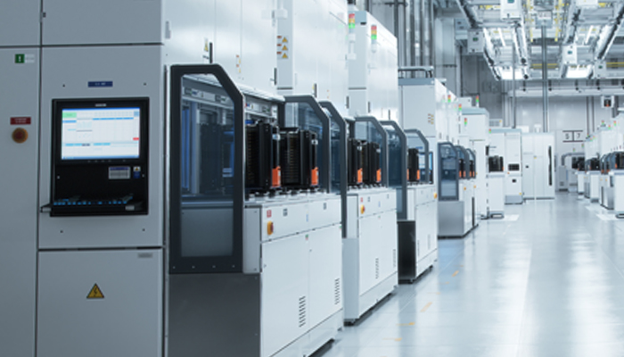
HYPERSCALE + CLOUD
The Speed of AI
224G interconnects and thermal management for next-gen compute nodes.

AUTOMOTIVE + EV
Power & Sensing
Heavy copper (>6 oz) and high-frequency laminates for ADAS and electrification.

NETWORKING + 5G
Signal Integrity
High-speed switch fabrication with optimized optical backdrilling.
SEMICONDUCTOR + OPTICAL
Reference Standards
Advanced fabrication for ATE, probe cards, and chip reference designs.