PATENT LICENSING
Partner Programs | Supplier Requirements
| Global Security | Supplier Engagement
INTELLECTUAL PROPERTY LICENSING
Sanmina Licensing of Patents and Intellectual Property
Sanmina has an extensive, worldwide patent portfolio associated with our work in several innovative technology and product sectors including PCB technology, surface mount technology, storage design, avionics and defense communications and memory solutions. Technology licensing opportunities available for consideration.
Technology Licensing – Simultaneous Via PartitioningTM (SVPTM )
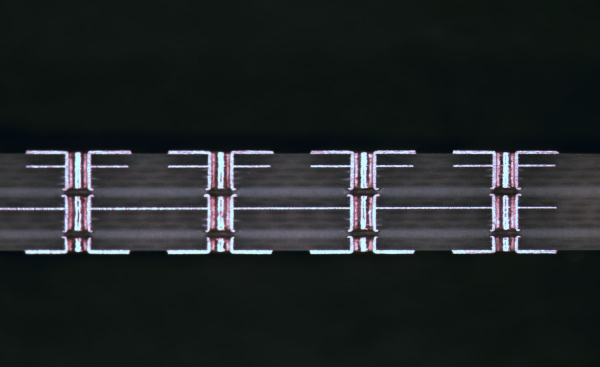
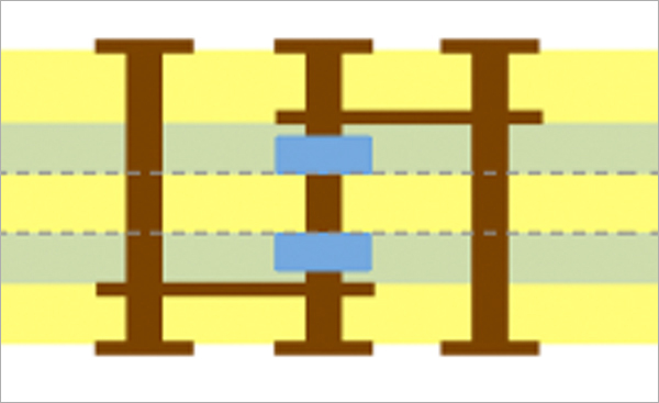
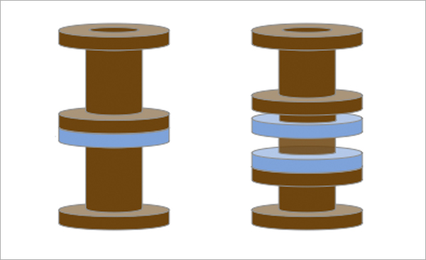
SVPTM technology is a patented PCB design that use a plating resist (PR) which selectively prevents copper plating and allows for a segmented via formation. This partitioned via results in the ability to significantly reduce or even eliminate stubs which would be left during the traditional PCB manufacturing process. Additionally, in certain designs, the segmented via created by this plating resist may be able to create opposing vias, normally only accomplished using a sub-composite approach, without the use of costly and time consuming multiple PCB lamination cycles.
Technology Licensing – Controlled Stub LengthTM (CSLTM)
Due to the precise nature of the SVP manufacturing process, each stub will be controlled via the design of the product, and will not be the result of the accumulated process tolerances of lamination (board thickness), drilling, and back drilling. These accumulated tolerances make it nearly impossible to build thick circuit boards in large form factors with a 6 mil maximum stub.
Technology Licensing – Zero Stub LengthTM
In situations where the full power of SVP is designed into the board from the start, it is possible that the resulting structure can achieve “Zero Stub Length”.