Vertically Integrated Wafer-to-Optical Systems Manufacturing
Accelerating 1.6T and CPO from Prototype to Turnkey Volume
Standard packaging methods hit thermal, RF, and physical density limits at next-generation speeds. Advanced Microsystems Technologies (A Sanmina Division) bypasses these barriers by merging microelectronic, optical, and RF design directly with volume manufacturing. We integrate bare die into MCM, SiP, Chip-on-Board, and CPO formats to scale complex silicon photonics from proof-of-concept to global hyperscale volume without re-engineering.
-
1.6T High-Density Transceiver Platform
-
Advanced Packaging and Integration
-
JDM Design and Development

Schedule a 30-Minute Conversation

Eric Sislian
GM & VP, Business Development and Strategy

Mike Newhouse
Product Development, Vice President of Engineering

Sid Sircar
Sr. Director of Optical Business Development

Cindy Snyder
Sr. Business Development Manager


1.6T HIGH-DENSITY
TRANSCEIVER PLATFORM
-
SiPh with Integrated Lasers Delivering Reliability and Power Efficiency
-
Simplified Architecture Maximizing Performance and Streamlining Assembly
-
Scale Out/Up Roadmap to 3.2T and Next-Gen Evolution
ADVANCED PACKAGING
AND INTEGRATION
-
Volume FlipChip and Chip-On-Board Capacity
-
Free Space and Guided Optical Assembly at Scale
-
Heterogeneous Integration of Bare Die, MCM, SiP, CPO
JDM DESIGN
AND DEVELOPMENT
-
Micro-Electronic, Optical, and RF Expertise
-
Proof-of-Concept to Turnkey Volume Manufacturing
-
Co-Located Design, Development, and Production
end-to-end cloud and ai infrastructure solutions

Validated Performance Across Multiple Industries

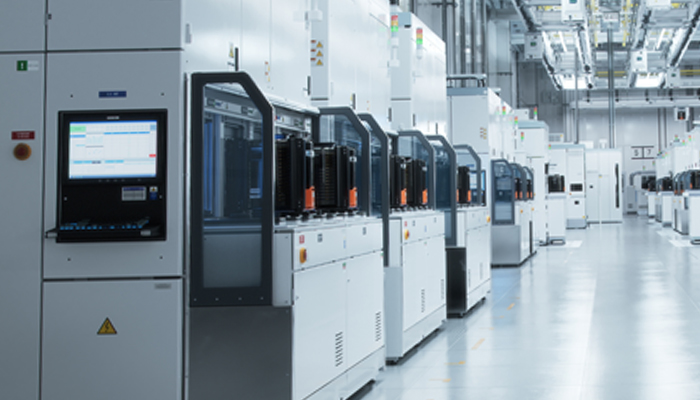
CLOUD AND AI DATA CENTERS

AUTOMOTIVE ELECTRONICS

COMMUNICATIONS NETWORKS
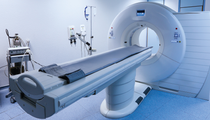
MEDICAL SYSTEMS
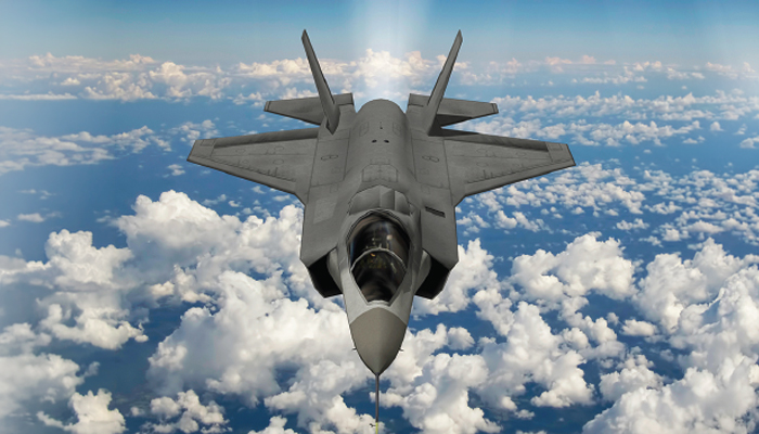
DEFENSE AND AEROSPACE
INDUSTRIAL SYSTEMS
Contact Us

