SANMINA TECHNOLOGY
Optical & RF Components • Printed Circuit Boards • Enclosures
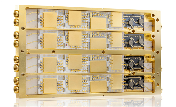
Sanmina’s Optical ,RF and Micro-electronics Division designs, industrializes and manufactures leading edge optical and RF devices using the latest in microelectronic assembly equipment optimized by our process engineers for your product.
Customers can choose from a wide range of service offerings. This flexibility enables our customers the opportunity to engage in the design and industrialization processes as much as or as little as they want while maintaining the product IP. All design services are performed with manufacturability and a robust supply chain in mind.
Printed Circuit Boards
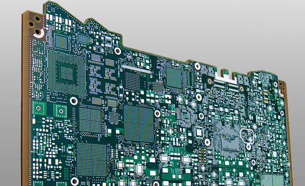
We partner with customers to develop custom, high-speed PCBs that deliver the highest performance in the industry using the latest technologies and materials, qualified in-house by Sanmina. Recent PCB innovations include:
- Blind/Buried/Stacked Via Escape Structures for Fine Pitch 3000+ Pin BGAs
- Multiple Sequential Laminations of Multiple Materials
- Castellated Slots for Direct Soldering of High-Speed Daughter Boards
- Embedded Passives
- Coin-in-Cavity Thermal Solutions
- Back Drilled Holes and much more
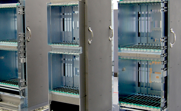
Enclosures
Customers benefit from Sanmina’s complete mechanical, thermal, and RF emissions design expertise for communications enclosure design, prototyping and production.
We offer design, DFX, prototype and volume production services for frames, racks and enclosures with hard and soft tooling, paint and powder coating.
Once the design is approved, Sanmina manages the transfer of manufacturing in order to provide the best total landed cost.
We also have extensive experience with fan tray, cooling and power system design.
Sanmina’s component technologies improve equipment performance and reduce costs for communications and network equipment customers. We offer a complete and integrated set of technologies for high-performance communications products including optical and RF transceivers, PCBs, backplanes and enclosures. We have in-house labs for materials analysis and signal integrity to qualify the latest high-speed laminates for PCBs and backplanes, as well as thermal and RF emissions labs for enclosures. Our design centers are located close to our customers, with best-cost manufacturing in all major regions worldwide.