DESIGN AND ENGINEERING
Optical & RF Components • RF & Circuit Design • PCBAs & Backplanes • Enclosures

Optical and RF Components
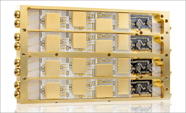
Sanmina designs and produces state-of-the-art optical and RF transceivers, modulators, amplifiers and other components.
Our customers retain the design IP, while Sanmina develops modules and subsystems incorporating the latest microelectronic packaging and substrate technology.
We offer customers complete services, including turnkey test system development for RF and optical systems.

RF and Circuit Design
Sanmina has design centers specializing in circuit and subsystem design for a broad range of communications products.
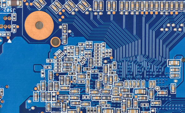
Product expertise includes RF and radio design, low noise amplifier design for communications and satellite applications, high speed digital electronics and power circuits.
Our combined experience with circuit design and high speed technologies such as RF, optical, PCB, cable and backplane technologies provides significant competitive advantage for our customers.

PCBs and Backplanes
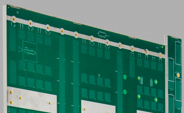
We develop custom PCBs that deliver the highest performance in the industry using the latest technologies and materials, qualified in-house by Sanmina. Recent PCB innovations include:
- Via escape structures for fine pitch 3000+ pin BGAs
- Advanced laminate qualifications, supporting low attenuation at 25 Gbs
- Backplanes: Multiple materials and sequential laminations
- Layer counts to 50+, panel sizes to 60 inches, blind connectors, backdrilling

Enclosures
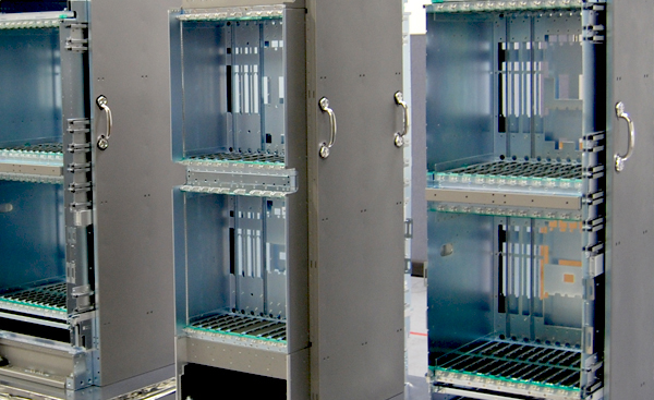
Customers benefit from Sanmina’s complete mechanical, thermal, and RF emissions design expertise for communications enclosure design, prototyping and production.
We offer design, DFX, prototype and volume production services for frames, racks and enclosures with hard and soft tooling, paint and powder coating.
Once the design is approved, Sanmina manages the transfer of manufacturing in order to provide the best total landed cost.
We also have extensive experience with fan tray, cooling and power system design.
Customers benefit from Sanmina’s decades of design experience for telecommunications components and subsystems including indoor and outdoor enclosures, PCBs, backplanes, cables, RF and optical components.
Our design capabilities are integrated; we can provide design or thermal, EMC and seismic analysis for an integrated backplane/enclosure subassembly.
We have in-house labs for materials analysis and signal integrity to qualify the latest high-speed laminates for PCBs and backplanes, as well as thermal and RF emissions labs for enclosures.


